
Plasma display panels are amongst flat panels those which reach the larger sizes. Currently the typical sizes of PDPs are diagonales between 30'' and 50'' with thicknesses of a few inches only and a total weight lower than 35 kg. That makes it really the TV that you can hang on the wall.
The main drawback of these devices for the TV market remains the high price. Today the cheapest PDP TV that you can find on the market costs around 4500$ for a 42'' diagonales.
There are two main reasons of this high cost: the first and major one comes from the price of the high power electronics required for sustaining electrical discharges in each pixels. The second source of expenses are the manufacturing costs of these devices.
The most important issue for the R&D in PDP is the luminous efficiency (i.e. the ratio between the useful light reaching the viewer and the injected electrical energy in lm/W). Currently the best luminous efficiency of comercialised PDPs is around 1.8lm/W as the luminous efficiency of cathodique ray tube is around 5lm/W.
Although 1.8 lm/W are already enough for the commercialisation, further improvements of the efficiency would help reducing the cost of the high power electronics.
Another important issue is the lifetime of PDPs even if it is now close to that of CRTs (around 30000 hours). The main source of limitations in PDP's lifetime is the sputtering of the materials covering the cathode (MgO) by ions from the plasma.
Finally research on the addressing time required for switching pixels into the ON state are also under way. In order to fit the video period requirement an elementary cells needs to be activated in less than 2 microseconds.
Mass production + R&D:
R&D in Europe:
If we try to depicted the different layers in a plasma display panels, at first we saw electrode strips deposited on the glass of the back plate.

Then a dielectric layer (~30 micrometers of ceramics with a relative permittivity around 12) is deposited above the electrodes.

On the dielectric layer, dielectric barriers (ribs) are patterned by sandblasting. These barriers separate the different address electrodes and are covered by phosphors in the three fundamentals colors.

The front plate is then sealed on these dielectric ribs. The front plate is again made of a glass plate on which are deposited pairs of electrodes X and Y. These electrodes (so called pairs of coplanar electrodes) are perpendicular to the address electrodes so that each intersections of address and coplanar electrodes we have one elementary cell. These coplanar electrodes are covered again by a dielectric layer. After this layer there is a thin layer of MgO (5000 Angström), the purpose of this layer is to protect the dielectric layer from the ions bombardment and in the same time it enhances the generation of secondary electrons at the cathode surface. After front and rear glass plates are sealed together the panel is pumped, baked out and re-filled with a mixture of inert gas (Xe with He or/and Ne) at ~ 400 Torr.
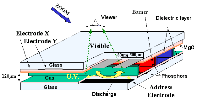
To switch ON one elementary cell a voltage is applied between two coplanar electrodes X and Y. This voltage will accelerate the seeds electrons in the gas and generate ions and excited particles: that is the plasma formation. The excited xenon atoms and molecules will deexcite by emitting VUV photons (yellow arrows on figure above). These V.U.V. will then strike the phosphors and converted into useful visible light (green, red and blue).
The purpose of address electrodes is to select the elementary cell which has to be turned on: during the addressing of the cell, the first discharge acts between one of the coplanar electrode and the address electrode (see figure below).

On the figure above, simulations of the addressing discharge (on the top) and of a sustain discharge (on the bottom) are represented. The simulated domain corresponds to one elementary cell (side view) of a PDP, the coplanar electrodes are on the left side.
One sustain discharge in a PDP elementary cell
When a PDP pixel is in the ON state, a succession of short electrical discharges (100ns) occurs in each of the three elementary cell of the pixel (one pixel is made of three elementary cell in the three fundamental colors).
As we saw before, the coplanar electrodes are covered by a dielectric layer so that an AC voltage needs to be applied to these electrodes. Typically a square wave voltage (100kHz, 400Vptp) is applied to the coplanar electrodes (see below) and a current pulse occurs at each half cycle of the applied signal. *
Now let's see why do we have short current pulses. At the beginning of a sustain cycle (position 1 on the figure) there are no charges above the dielectric which covers the coplanar electrodes.
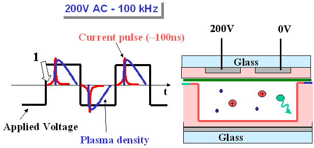
Due to the applied 200V the seeds electrons already present in the cell volume begin to strike the atoms of the gas (Xe, Ne and He) to form new ions and electrons (and also excited particles which will emit the necessar UV photons).

This electron avalanches leads to an increase of the current (rising part of the current pulse). In the same time that charges are created in the volume they are collected on the dielectric which cover the electrodes. Ions will charge the dielectric area above the cathode and electrons will be collected above anode. This lead to a wall-charge above each electrodes and thus to a wall-voltage which is opposited to the applied voltage.
In consequence the voltage accross the gas (Vgas= Vappl. - Vwall) will decrease with the accumulation of charge on dielectric (we are then on position 2 of figure above). As the voltage across the gas diminishes the ionisation also diminishes and the current decrease.

When enough charges are collected above each electrodes so that the voltage accross the gas equal 0, the current becomes also equal to zero (position 3 on figure above, Vappl.=Vwall).
The coplanar electrodes are transparent to the visible light (Indium Tin Oxyde). To ensure the conductivity all along these electrodes strips, a smaller metallic strip is added on the edge of the ITO strips. The ITO layer is deposited by a sputter deposition method and there are patterned by a photolithographic etching.
The same methods are used to design the address electrodes on the rear glass of the PDP.
2. Dielectric layers (er~10-20): Screen Printing (580°C)
The dielectric layers above the
electrodes are deposited by a screen printing method (thick layers
around 30 micrometers). The dielectric is then dryed at 580°C so that
the glass plates needs to sustain such a high temperature.
To make the barrier ribs, a very thick layer (>100 micrometers) is deposited by screen printing and dryed at 580°C . The pattern of the ribs (barriers, waffle structure, ...) is then made by a sand-blasting etching method.
On the front plate the dielectric covering the coplanar electrodes is protected by a thin layer of MgO (magnesium oxyde) against the energetic ions and neutrals. This layer is deposited by the evaporation of MgCO3 under an electron beam (MgCO3 -> MgO + CO2).
The phosphor layer is deposited by a screen printing method on the rear plate of the panel.
The front and rear plates of the panel are sealed together by melting a frit (which melt at 450°C) deposited on the edge of the panel. Some holes are left open in order to pump the panel during a long baking period (several hours at temperatures around 400°C) and also for injecting the new gas mixture contening the Xenon.